Table of Contents
- What is Cache?
- What is CPU Cache or CPU Cache Memory?
- CPU Cache Vs. Other Memory Units
- What is the CPU Cache's Significance in a Processor?
- How Does CPU Cache Memory Work?
- Types of CPU Cache
- How L1 and L2 CPU Caches Work
- CPU Cache Memory Mapping
- Data Writing Policies
- Locality
- The Future of the CPU Cache
- Conclusion
When the nano-dimensional semiconductor industry offers a golden period for CPU hardware development, essential components like CPU cache are not lagging far behind to utilize the opportunity in all possible ways. Nano-range transistors leave enough space for the CPU cache to follow in the same footsteps of advancement. Since information processing starts with accessing the data, the modernization of the CPU cache plays a vital role in the overall performance of a microprocessor. These days, it is sufficient to say that we all have heard about CPU cache memory while buying a computer or discussing the CPU. The invention of the CPU cache was a significant event in the history of computers. It was to solve a severe problem with CPU performance. Earlier processors were bound to access data from the system memory. However, advancements in CPU technology were calling for high-speed data access systems since the main memory could not cope with its performance. Here, CPU caches play their part in traversing the performance gap between these two components. Let us take you on a journey to describe how the story started. Stay tuned. We will begin with the concept of caching first.
What is Cache?
In computer literacy, the word 'cache' refers to a temporary data storage component prepared to serve future requests for that data. The cache is used for both hardware and software purposes. But why do we need them? They are faster to respond than the primary storage section. Cache data is created mainly due to the previous computation or a copy of some essential data stored elsewhere.
What is CPU Cache or CPU Cache Memory?
Cache memory should not be confused with the general term cache. It is the hardware implementation of memory blocks that the CPU uses to create cache data from the main memory. These data blocks are born when various programs run and make a copy of their recent information so that the CPU can access them more efficiently next time, matching the CPU clock speed. The chip-based cache memory is also called CPU cache memory since it is mainly integrated with the CPU chip or directly connected through an interconnecting bus. Simply put, the CPU cache is the most quickly accessible memory unit. It helps to improve the CPU access speed.

CPU Cache Vs. Other Memory Units
As we already know, at least three types of physical memory sections exist in a computer memory hierarchy.
CPU Cache vs Primary Storage:
-
Primary storage refers to the HDD or SSD, a memory unit, and a storage system. It stores a bulk amount of data, including the OS and other programs. Unlike the other memory units, the storage technology is non-volatile, meaning it doesn't lose its content without a power supply. It's a computer's most extensive, slowest, and inexpensive memory section.
CPU Cache vs The System memory:
-
The system or main memory refers to the RAM or Random Access Memory. It runs on Dynamic RAM or DRAM technology and is implanted on the motherboard. This limited memory unit is volatile and less expensive than the CPU cache. This larger RAM unit provides half of the speed of a CPU cache memory, although it's faster than the primary storage.
CPU Cache vs Virtual Memory:
There is also a memory type named virtual memory, but this is not a memory block but a technique to enhance the RAM capacity so that the ability to run more extensive programs or multitasking capability of a computer increases. Yet, regarding accessibility speed, this memory technique is also slower than the CPU cache memory.
Computer memory hierarchy based on size and data access speed[/caption]
Lastly, we come to the CPU cache. It is also RAM, but the hardware used here is Static RAM or SRAM. It is made of CMOS technology with six transistors for each cache block, whereas DRAM uses capacitors and transistors. Due to charge leakage, DRAM is required to be refreshed continuously to retain data for a more extended period. Hence, it consumes more power while providing slower memory access. However, SRAM doesn't require refreshing to store data for a long time. Although SRAM is more complex and expensive, it empowers the CPU cache memory to respond to a CPU request in a few nanoseconds only.
Read Also: How to Stop System Data Usage in Windows 10
What is the CPU Cache's Significance in a Processor?
In the early days of computing, when CPUs were not fast enough, the main memory could cope with its velocity. After 1980, the velocity gap between CPU and RAM started to widen significantly with the advancement of processor cache technology.
CPU-DRAM speed gap[/caption]
As the microprocessor clock speed grew, the RAM access time couldn't reach a similar level. Hence, the RAM became responsible for pulling the CPU performance behind. In this scenario, the demand for faster memory gave birth to the CPU cache system. Currently, mainstream consumer CPU clocks run around 4GHz velocity, whereas most DDR4 memory units reach up to 1800MHz speed. The main memory is undoubtedly too slow to work directly with the processor. The CPU cache memory plays the most significant role in bridging the velocity gap between the RAM and the processor for the CPU to perform efficiently. CPU cache works as an intermedial buffer between these two. It stores small blocks of repeatedly used data, or sometimes, only the memory addresses them.
Comparing different memory performance[/caption]
The significance of the CPU cache memory is in its efficiency in data retrieval. Fast access to the instructions enhances the program's overall speed. When time is the essence of this modern world, even a few milliseconds of more latency could potentially lead to gigantic expenses based on a specific situation.
Read Also: How To Troubleshoot and Fix Blue Screen?
How Does CPU Cache Memory Work?
Let's take an example of a program. It is designed with instructions to be controlled by the CPU (how does cache work). Now, the program is loaded in the primary storage. Therefore, when the program is launched, the instructions snake through the memory hierarchy toward the CPU. The instructions get loaded into the RAM from the primary storage and then reach the CPU. Modern CPUs can now bear a large chunk of data per second. However, the CPU requires access to a high-speed memory module to utilize all its power. This is where the cache starts playing. The memory controller loads the data needed from RAM into the store. Based on the CPU design, this controller can sit inside the CPU itself or on the North Bridge chipset on the motherboard.
Data flow across the CPU, cache memory, and main memory
Lastly, the data is distributed inside the cache depending on the memory hierarchy to carry it back and forth inside the CPU. Now, CPU caches act like small memory pools to store the most probable information the CPU requires at the next moment. There are sophisticated algorithms to determine which programming code will be needed next and hence to be loaded in the first layer of CPU cache memory and then in the other layers. The very purpose of the cache memory is to feed the CPU immediately as it calls upon a request so that the CPU can work around the clock without much lagging.
Read Also: Tips to Take Care of Your Laptop During Summer | How to Take Care of Your Laptop
Types of CPU Cache
Generally, CPU cache memory is divided into three primary levels: CPU cache l1, l2, and l3. The ranking is marked according to decreasing CPU cache speed and closeness to the CPU l1 l2 l3 cache size and hence the increasing size of the layers as well; here in this, we also share what is the trade-off between size and speed between l1 and l2:
L1 Cache:
The l1 cache, which means Level 1, represents the primary cache, the fastest memory block in a computer. This minor section in the li cache generally comes embedded in the microprocessor chip. How l1 store works → According to access priority, the L1 cache retains the data most likely to be retrieved by the CPU up next to finish a specific task. Generally, the L1 cache size (l1 cache memory size) ranges from 256 KB to 512KB for flagship processors while offering 64KB for each CPU core. However, some power-efficient CPUs are currently implanting it close to 1MB or more. Server chipsets like Intel's Xeon CPUs have 1-2MB of L1 cache. The L1 cache is split into the L1 Instruction and the L1 Data Cache. The instruction layer retains the commands the CPU has to perform to run the operation, and the data cache keeps the data to be written back to the main memory. The instruction cache also holds pre-decode information and branching data. The data cache often acts like an output cache, whereas the instruction cache is an input cache. This circular process is helpful when loops are involved in a specific program. In earlier processors, when the L3 cache was not included, the system RAM was used to communicate directly through the L2 cache: RAM → L2 Cache → L1 Instruction Cache → Fetch Unit → Decode Unit → Execution Unit → L1 Data Cache → RAM. An Intel Sky Lake CU cache design showing cache memory arrangement
L2 Cache:
What is the l2 cache → The secondary cache is more extensive but slower than the L1 cache. This one may be embedded in the CPU or set on a separate chip or a coprocessor. In the latter case, an alternative high-velocity system bus connects the cache with the CPU so that it doesn't lose efficiency due to the traffic on the main memory bus. L2 cache ranges from 4-8MB on flagship processors (CPU l2 cache size 512KB per core), although you can expect even more of it in modern power computers. Generally, in modern multicore CPUs, we see each core's dedicated L1 and L2 caches embedded in them, whereas the L3 cache is shared across them all.
L3 Cache:
The third level is specialized in improving the performance of L1 and L2. Although L1 and L2 are significantly faster than L3, L3 can churn out double the speed of DRAM. The size of the L3 cache can vary from 10-64MB. Server chips can go up to 256MB of L3 cache. AMD's Ryzen CPUs have recently been implanted in many larger stores than their Intel counterparts. Earlier, the trend was to create L1, L2, and L3 caches using a combination of processor and motherboard components. Currently, the tendency of consolidating all three levels of cache memories on board with the CPU is gaining popularity.
Contrary to popular belief, implanting extra DRAM won't increase cache memory. Sometimes, two expressions, ' memory caching' and 'cache memory,' are often used synonymously, but they are different. Memory caching is a DRAM or flash memory process to buffer disk reads to enhance storage I/O performance. Meanwhile, cache memory is a physical memory unit that provides read buffering for the processor.
Also Read: Best SSD for Laptop? Learn The 7 Best Ways to Choose It.
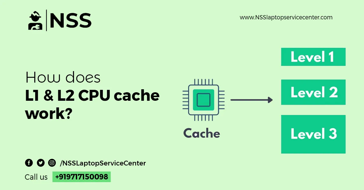
How L1 and L2 CPU Caches Work
The data flow snakes through the RAM to the L3 cache, reaching the L2 and L1. When the processor searches for data to operate, it first looks into the associated core's L1 cache. If the data is found there, the situation is called a cache hit. Otherwise, the CPU scampers arch for the data in L2 and then L3 caches. If it can't find the data, it tries to retrieve it from the main memory. This condition is called a cache miss. In that case, the CPU must request that it be written onto the cache from the RAM or storage. This process consumes time and negatively affects performance. The cache memory performance is frequently measured in the Hit ratio. Hit ratio = no. of hits / (no. of hits + no. of misses) = no. of hits / total accesses. Generally, the cache hit rate improves with increased cache size. The effects are considerably visible in latency-sensitive workloads, such as in gaming. Latency is defined by the time required to access data from a memory unit. Resultantly, the fastest L1 cache has the lowest latency, and then it increases according to the cache hierarchy. In the case of a cache miss, the latency increases a lot since the CPU has to retrieve information from the main memory. Let's take an example.
Suppose a processor has to retrieve data from the L1 cache 100 times in a row. The L1 cache has a 1ns(nanosecond) access latency and a 100 percent hit rate. Resultantly, the CPU will take 100ns to perform this operation. Imagine that the cache hit rate is 99 percent, and the required data for the 100th access is in L2, with a 10ns access latency. Therefore, the CPU will take 99ns to play the first 99 reads and 10ns to perform only the 100th. This means that a 1 percent depletion in hit rate slowed the CPU by 10 percent. In actual practice, an L1 cache shows a hit rate within 95 to 97 percent, but the performance impact between these two values can differ by around 14 percent if the remaining data sits in the L2 cache. But if it's a cache miss and the data is in main memory, with 80-120ns access latency, the CPU may take nearly double the time required. As computers evolve, latency decreases as well. Low-latency DDR4 RAM and high-speed SSDs significantly reduce a computer system's overall latency. Earlier cache designs were made so that L2 and L3 caches used to be kept outside the CPU chip. This process was causing more latency due to the distance of the cache units from the processor. However, the current fabrication processes ensure the insertion of billions of CPU transistors in a relatively minor space, Thu, leaving more room for the cache unit. As a result, the closeness of the cache to the CPU is growing, and the latency is lowering. That's why the market focus has shifted from buying a computer with a large cache size to one with sufficient integrated cache levels with the CPU chip.
Read Also: Best Way to Troubleshooting Keyboard Backlight Failure
CPU Cache Memory Mapping
This process explains how the CPU cache communicates with the main memory. The cache memory is split into blocks. Again, each block can be divided into n 64-byte lines. The RAM is also divided into blocks that interact with cache lines or sets of strings. A coalition of memory can't be placed randomly into the cache. The restriction is confined to one cache line or a group of cache lines. The cache placement policy determines where a specific memory block can be put into the cache. Although caching configurations are evolving continuously, three different policies are traditionally available for placing a memory block into the store.
Direct Mapping:
In this process, the cache is split into multiple sets, having one cache line per set. According to the memory block address, each block is mapped to precisely one cache memory line. The cache can be represented as an (n*1) column matrix. The set is recognized by the index bits of the memory block address, and a tag with all or part of the address of the data is stored in the tag field. The new data rewrites the allocated place in the cache if the given area is occupied.
Direct-Mapped Cache[/caption]
The performance of this most straightforward process is directly proportional to the hit ratio. It is power-efficient since searching through all the cache lines is unnecessary. And because of its simplicity, it doesn't require expensive hardware manufacturing. However, the hit rate here is low because there is only one option for each data block, and the search increases cache misses.
Read Als is unnecessary: How to Fix Distortion and Discoloration of Your Laptop Screen.
Associative or Fully-Howeverive Mapping:
This process arranges The cache into a single set with multiple lines. A memory block can inhabit any of the cache lines. The arrangement can be represented as a (1*m) row matrix.
Fully Associative Cache[/caption]
This process offers a hit rate. Also, various replacement algorithms can be applied here if the cache miss occurs. However, the process is slow since each search goes through the entire cache and is power-hungry for the same reason. Moreover, it requires the most expensive associative-comparison hardware among all three policies.
Set-associative Mapping:
This process can be seen as an improved version of direct mapping. More precisely, it's a trade-off between the other two. A set-associative cache can be framed as an (n*m) matrix. The store is split into n sets; every pack contains m lines. A memory block enters a group and then occupies any cache line.
[caption id="attachment_13030" align="aligncenter" width="578"]
Set-Associative Cache[/caption]
A direct-mapped cache can be imagined as a one-way set-associative, and a fully associative cache with n cache lines can be seen as an n-way set-associative. Most contemporary processors inherit either a direct-mapped or a two-way or four-way set-associative configuration.
Data Writing Policies
Although various techniques are available, two central writing policies are under which cache memory is written.
Writinherita is written to both the cache and a backing store (another cache or main memory) at a time.
Write-back (or Write-behind):
-
Initially, data is written only to the cache. Reporting to the backing store occurs only when the present data is about to be replaced by another data block.
The data writing policy directly impacts data consistency and access efficiency. If it's a write-through process, more writing must be done, which causes latency upfront. In the case of a write-back policy, efficiency may be enhanced, but data directly impacts between the cache blocks and the main memory.
Locality
This concept also has a significant influence on a computer's overall performance. Locality determines various conditions to make a system more predictable. The CPU cache memory considers these situations before it creates a pattern for data retrieval that it can rely upon. Among the several types of them, two basic ones are described here:
Temporal locality:
-
In this case, the same resources are used repeatedly in a short period.
Spatial locality:
-
In this one, data or resources are accessed from the resources which are near each other.
The Future of the CPU Cache
The research on CPU cache memory is now advancing more than ever. As well as the experiments focusing on cutting-edge CPU models, CPU cache designs are also trying to match the same footsteps of churning out the best performance of smaller and cheaper structures. Manufacturers like Intel and AMD are not only competing on larger cache designs with higher L4 levels, but we are also getting a trim L0 cache level in some modern processors. Although the latter is now only a few KB in size, they are made for CPUs to access these tiny data pools easily with even lower latency than the L1 cache. Undoubtedly, a lot is going on to remove the bottlenecks on modern computers. One aspect is vowed to develop the best solutions for latency reduction; another is dedicated to fitting larger caches onboard with the CPU chips or experimenting with hybrid cache designs. Whatever it is, it looks like the future of the CPU cache market will offer us surprising performance out of mainstream computers. In today's discussion, we tried to provide some basic information on the CPU cache memory work procedure. If you still have questions, please get in touch with us anytime. We are here for you, always.
Here is the List of Dell Authorised Service Centers in Mumbai | HP Authorised Service Centers in Mumbai
Conclusion:
Since retrieving data from the l1 cache and l2 cache is the first step in information processing, modernizing the CPU cache is crucial to a microprocessor's overall performance (the performance of cache memory is frequently measured in terms of a quantity called hit ratio, which is calculated as). A significant development in the history of computers was the creation of the CPU cache. This blog is all for you if you think about how much cache memory suits a laptop or about l1 and l2 cache memory. The memory blocks utilized by the CPU to construct cached data from the main memory are implemented in hardware. CPU cache compared to system memory: Random Access Memory, sometimes known as RAM, is called the system or main memory. CPU Cache vs. Virtual Memory: Virtual memory is another sort of memory, but it isn't a memory block; instead, it's a method for expanding RAM so that a computer can execute more complex programs or perform many tasks simultaneously.
Here, the CPU cache memory performs the most crucial part in bridging the speed gap between the processor and RAM so that the CPU can operate effectively. The data cache stores the data that will be written back to the main memory, whereas the instruction layer stores the orders the CPU must execute to complete the process. The latency dramatically increases since the CPU must obtain data from the main memory in case of a cache miss. As a result, the latency decreases, and the cache's proximity to the CPU increases.
Frequently Asked Questions


Popular Post
- HP Laptop Keyboard Backlight Not Working
- What's The Best Laptop Repairing Center In Noida
- Top 5 HP Printer Repair Service Center Provider In Delhi
- Wifi Not Working On Windows 10
- Lenovo Flex 3 Screen Replacement & Repair: Cost, Issues & Best Service
- How To Make A Video Call From Laptop To Mobile
- Right Click Shortcut
- How Do I Fix The Horizontal White Lines Appearing On My Laptop Screen
- Lenovo Laptop Is Not Charging Issue
- How To Repair And Restore Windows 10 On Hp Laptop
Categories
NSS Laptop Service by Location
Popular Services
- MacBook Battery Replacement Cost
- HP Printer Repair in Delhi NCR
- Dell Laptop Repair
- HP Laptop Repair
- Samsung Laptop Repair
- Lenovo Laptop Repair
- MacBook Repair
- Acer Laptop Repair
- Sony Vaio Laptop Repair
- Microsoft Surface Repair
- Asus Laptop Repair
- MSI Laptop Repair
- Fujitsu Laptop Repair
- Toshiba Laptop Repair
- HP Printer Repair Pune
- Microsoft Surface Battery Replacement
- Microsoft Surface Screen Replacement